The Future of Silicon Solar Cells: Beyond Traditional Architectures
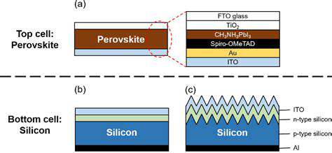
Perovskite-Silicon Tandem Cell Efficiency
Perovskite-silicon tandem solar cells represent a significant advancement in photovoltaic technology, aiming to surpass the efficiency limitations of single-junction silicon cells. Their unique structure, combining the high light absorption of perovskite materials with the established stability and manufacturing processes of silicon, offers a promising path towards higher energy conversion efficiencies. This combination allows the tandem cell to absorb a broader spectrum of sunlight, thereby capturing more energy than a single-junction cell.
The key to this enhanced performance lies in the complementary absorption characteristics of the two materials. Perovskite excels at absorbing shorter wavelengths, while silicon excels at longer wavelengths. By strategically layering these materials, the tandem cell can harvest a greater proportion of the solar spectrum, ultimately leading to a substantial increase in the overall energy conversion efficiency compared to traditional solar cells.
Challenges in Tandem Cell Development
Despite the significant potential, several challenges hinder the widespread adoption of perovskite-silicon tandem solar cells. One major hurdle is the fabrication process, which often requires precise control over the deposition of the perovskite layer on top of the silicon substrate. Maintaining consistent layer thickness and minimizing defects is critical for optimal performance and scalability. This intricate process demands advanced fabrication techniques and sophisticated control mechanisms.
Another critical challenge lies in the stability of the perovskite layer under real-world operating conditions. Exposure to moisture and oxygen can degrade the perovskite material over time, leading to a decline in the cell's performance. Developing robust passivation strategies and improving the overall stability of the perovskite layer are essential for long-term performance and commercial viability. Addressing these stability issues is vital for widespread acceptance and integration into large-scale solar energy systems.
Future Applications and Market Potential
The potential of perovskite-silicon tandem cells extends beyond simply enhancing solar energy efficiency. Their high efficiency and relatively low cost compared to other advanced technologies position them as a strong candidate for various applications, including building-integrated photovoltaics and large-scale solar farms. The ability to achieve higher power conversion efficiencies opens up new avenues for cost-effective energy production and addresses the critical need for sustainable energy solutions.
The market potential for perovskite-silicon tandem cells is substantial. As research progresses and challenges are overcome, these cells are expected to play a significant role in the transition to a cleaner energy future. The potential for significant cost reductions and improved performance makes perovskite-silicon tandem cells a highly promising technology for the future of solar energy. Government support and investment in research and development will be instrumental in accelerating the commercialization of this technology.
Silicon Nanowire Arrays: Capturing Light with Precision
Silicon Nanowire Arrays: A Novel Approach to Solar Energy Harvesting
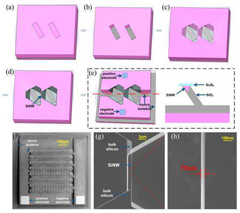
Silicon nanowire arrays are a promising new technology for solar energy conversion. These arrays offer a unique approach to light absorption, significantly increasing the efficiency of solar cells compared to traditional flat-panel designs. The nanowire structure creates a large surface area for light interaction, leading to enhanced light trapping and improved charge carrier collection. This translates into greater power output from a given area of solar panel.
A key advantage of silicon nanowire arrays lies in their ability to absorb a broader spectrum of light compared to conventional solar cells. This broadened absorption spectrum allows the devices to utilize a greater portion of the solar spectrum, thereby increasing overall energy conversion efficiency. Moreover, the unique geometry of the nanowires facilitates the efficient separation and collection of photogenerated electron-hole pairs, a crucial step in the photovoltaic process.
Fabrication and Characterization: Key Aspects of Development
The fabrication process for silicon nanowire arrays is a critical aspect of their development. Precise control over the nanowire diameter, length, and density is essential for optimizing performance. Various techniques, such as chemical vapor deposition (CVD) and electrochemical etching, are employed to create these intricate structures. Careful selection of these techniques and parameters is crucial to achieving the desired performance characteristics.
Thorough characterization of the nanowire arrays is necessary to understand their structural and optical properties. Techniques like scanning electron microscopy (SEM) and transmission electron microscopy (TEM) are used to visualize the nanowire morphology and confirm the desired dimensions. Further analyses, such as photoluminescence spectroscopy and current-voltage measurements, are essential for evaluating the electrical properties of the fabricated arrays and for identifying any performance limitations or defects.
Advanced characterization methods are critical for understanding the relationship between the nanowire structure and the overall device performance. This detailed understanding guides further optimization of the fabrication process and material properties for enhanced efficiency.
Applications and Future Directions: Beyond Solar Energy
Beyond solar energy harvesting, silicon nanowire arrays show promise in various fields, including biosensing, catalysis, and high-density electronics. Their unique properties, such as high surface area and tunable optical characteristics, make them attractive candidates for these applications. For instance, the highly sensitive nature of these structures could be leveraged in biosensors, allowing for the detection of minute amounts of biological molecules.
The future of silicon nanowire arrays looks promising, with ongoing research focusing on improving their performance and exploring novel applications. Researchers are actively investigating ways to enhance light absorption, improve charge carrier transport, and reduce manufacturing costs. These advancements hold the key to unlocking the full potential of this innovative technology in diverse applications.
Further research is needed to understand the long-term stability and reliability of these nanowire arrays in various environments. This long-term stability is critical for the widespread adoption of these devices in applications like solar energy generation.
Read more about The Future of Silicon Solar Cells: Beyond Traditional Architectures